Introduction
Optical integrated circuit is a device that integrates multiple photonic functions to perform certain operations on an optical signal. Unlike electronic integration where silicon is the dominant material, Optical integrated circuits can be fabricated from various materials such as crystals, silica and
other kind of polymers and semiconductor materials. Various use of these materials and fabrications gave many advantages many fields in industry. Integrated optics is a huge topic which includes numerous applications in different areas. Integrated optical detectors and integrated semiconductor lasers are some of them.
Integrated Optical Detectors
Optical Detectors, also known as Photodetectors are structures which can convert a light into an electrical signal. They are the fundamental elements of many optical systems such as optical power measurement and receiver modules of the fiberoptic communication systems. The simplest type of an
optical detector is photodiodes. Various integrated structures and different application of photodiodes can be included under the subject of integrated optical detectors. These components
and sensors are used in many industrial areas such as medical sensing and robotics. These structures have different production methods, working principles and usage areas. Some of the important parameters that characterize photodetectors are sensitivity and responsivity. Photodetectors can be subdivided by the physical effects and detector response types. Photodetector types can be examined under subjects like photocondutive, photovoltaic, and photoemissive.
Photoconductive Detectors
The catched light generates electrons which carry electrical current so the conductivity of the detector material changes proportional to the intensity of the coming light. Photoconductive detectors are fabricated from semiconductor materials like silicon.
Photodiodes
Photodiodes are designed to detect light particles called photons to be used to detect light and measure the intensity. Phototransistors are internal amplified photodiodes.
A photodiode acts as a photo-controlled current source in parallel with the semiconductor diode. Basically, a photodiode is a current generator. If light falls on the photodiode, the reverse current begins to flow. If the photons stimulate the carriers in a reverse-biased pn junction, a very small current flows over the diode with proportional to the intensity of the light.

Current through photodiodes is directly proportional to the intensity of the light. Light sensitivity to the wavelength is illustrated in figure above.
A photodiode acts as a photo controlled current source in parallel with the semiconductor diode and can be examined with the standard diode equation where Ip is the photocurrent.
+I_{p})
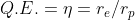
The ability of a photodiode to convert light energy into electricity is measured by Quantum Efficiency. η is the ratio between the number of electrons collected as Ip/sec and number of incident photons/sec. Efficiency also depends on absorption coefficient, thickness, doping, temperature, geometry, etc.
Responsivity of the photodiode Rλ defined as the ratio of output current in amperes to the radiated energy in watts. (A/W)

Responsivity of the photodiodes with different materials under different wavelenghts of light can be seen in figure below.

p-i-n photodiode widely used across different applications because of its simple structure which makes its cost efficient. But for more precise applications on industry or academic research, under ideal conditions and high quality materials design with Q.E. of 80% can be accessed.
Infrared Sensors
Infrared light contains less energy per photon compared to the visible light band. For this reason, an infrared photon often lacks the energy required to trigger the detection threshold of a photodetector. Infrared is often measured using a thermal detector, such as a thermopile, which is a heat sensitive device that measures radiated heat.
These detectors have flat spectral sensitivity, but they struggle from temperature sensitivity and often need to be cooled with an external structure. Before incoming light approaches the thermal detectors light modulated with a chopper. This method makes it possible for the thermal detector to measure the difference between light and dark.
Since heat means basically an infrared light radiation, thermal detectors are sensitive to environmental changes Night vision equipments takes advantage of this effect to distinguish people in the dark.
Infrared is much more difficult to manage than visible light. It is harder to focus an infrared light with lenses, because the refractive index varies with wavelength and creates dispersion.
Photovoltaic Detectors
This type of detectors contains a pn junction. Voltage is generated when light energy captured.

Photovoltaic Cell
A photovoltaic cell is made from semiconductor materials which can absorb the light particles and generates an electron flow to the circuit. When a photon hit a semiconductor material like silicon, it releases an electron from its atom. The free electrons move and fill a electron hole. But electrons must flow in the same direction, not randomly, in order to produce a current on the circuit. In order to achieve this two different types of silicone used. The layer with the surface facing to the light is doped with phosphorus which have more electrons than silicon or boron doped sides. This sandwich structure is similar to a battery. The layer with more free electrons becomes negative terminal (n) and the other layer with less free electrons becomes positive terminal (p). At the junction between these n and p layers an electric field is created. When electrons are triggered by photons, the electric field is goes to the n layer while the holes are goes to the p layer as seen in the figure above.
Photoemissive Detectors
These detectors are supported the photoelectric effect, within which incident photons release electrons from the surface of the detector material. Then free electrons are collected in an external circuit.
Integrated Semiconductor Lasers
A laser diode is a semiconductor device similar to a light-emitting diode (LED) which triggered by electrical current. Lasers can convert electrical energy directly into light. There are two types of photon emission. Spontaneous emission which under a voltage difference, the doped p-n junction allows for recombination of a hole with lower energy level an electron with higher energy level in the form of an emitted photon radiation. And stimulated emission which produces when this process is triggered with an initial photon to generate another photon with the same wavelength and phase.
The semiconductor material choice determines the emitted beam wavelength, which changes between IR to UV on light spectrum. Semiconductor laser diodes are the most common type of lasers in todays production. They used in a wide range of areas such as laser pointers, fiber optic communications, scanning, printing, and barcode readers.
Semiconductor laser diodes are fabricated from direct band gap materials, using elements from groups 3 and 5 in the periodic table, such as aluminum (Al), arsenic (As), gallium (Ga), indium (In), and phosphorus (P). Diode lasers have high efficiency and capable of high power outputs.
Double Heterostructure Lasers

In double heterostructure semiconductor laser diode, a narrow band gap material layer like gallium arsenide (GaAs) is placed between the two high band gap layers like aluminum gallium arsenite (AlGaAs). It is called the “double heterostructure laser” aka. DH laser because both of the junction points between the layers is called a heterostructure.
One of the advantages of the double heterostructure laser is the region of the free electrons and holes exist at the same time which called the active region is limited with the middle narrow band gap material layer. This means, more electron-hole pairs can stimulated to enable the amplification. But the generated light is limited to the region where the amplification happens.
Quantum Well Lasers

In Quantum Well Lasers, middle layer is thin enough to acts as a quantum well which means the output energy boosted because of the electron’s wave function. The efficiency of a quantum well laser is better than a solid state bulk lasers with crystals because the density of the electrons in the quantum well.
Separate Confinement Heterostructure Lasers

One of the disadgentages of the quantum well laser diode is that the thin layer is too small to effectively restain the light. To compensate, another two layers are added outside. These layers have a lower refractive index than the layers inside, so restain the light more efficiently. This design is called a separate confinement heterostructure (SCH) laser diode. Almost all of the commercial laser diodes after 90s have been separate confinement heterostructure quantum well diodes.
Vertical-Cavity Surface-Emitting Lasers

Vertical-cavity surface-emitting lasers (VCSEL) have optical gap along the direction of the current flow, not perpendicular to the direction if the current flow, as in conventional laser diodes. The active zone size is shorter than the side dimensions, thus radiation exits from the surface of the cavity, not from the edge of it just like in the figure. There are upper and lower reflectors at both ends of the cavity using dielectric mirrors with an alternative high and low refractive index.
Those dielectric mirrors provide a high degree of wavelength selective reflection but, because of their high mirror reflectivity, vertical-cavity surface-emitting lasers have lower output power compared to edge-emitting lasers.
Acknowledgment
I would like to thank my advisor Associate Professor Onur Ferhanoğlu.
References
-
Hunsperger, Robert G., Integrated Optics: Theory and Technology, Springer Berlin Heidelberg, 2002.
-
Wei-Chih Wang, Optical Detectors, Department of Power Mechanical Engineering, National Tsing Hua University.
-
Coldren, L.A. and Corzine, S.W. and Mashanovitch, M.L., Diode Lasers and Photonic Integrated Circuits, Wiley, 2012.
-
Sala A., Integrated Photonics, OP-TEC, 2016.
You can access to the real paper from here.